M3966m Mosfet Verified [work] Jun 2026
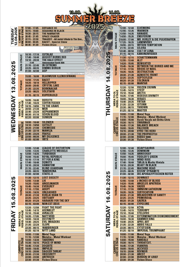
Running Order (PDF / Excel)
 PDF onepager
Maps

Click on the graphic to view the festival site plan as a PDF.

Click on the graphic to view the infield site plan as a PDF.
Legal guide agreement
Click HERE!
Packing list

Have you encountered this specific marking in your repairs? Did the pinout match the standard SO-8 configuration? Let us know in the comments below to help build the community database!
It is a widely utilized component in electronics repair and manufacturing, typically found in compact surface-mount packages. 🔍 Key Specifications
Housed in a larger, thermally superior DFN5x6 (PRPAK5x6) footprint.
Set your multimeter to (symbol →+).
Switching test (resistive load, VDD=30V, ID=6A):
Verify if your board layout calls for the M3 size profile (3x3mm) or M6 profile (5x6mm). They cannot be interchanged on the PCB track due to size differences.
. It is widely used in power management circuits, particularly as a switching regulator in laptops and computer motherboards, including many Key Technical Specifications m3966m mosfet verified
The (often labeled as QM3966M ) is a high-performance 30V N-Channel MOSFET typically manufactured by uPI - UBIQ . It is widely used in high-frequency switching power supplies, DC-DC converters, and motherboard power management, such as in Asus laptops . Key Specifications
Employs a broader 5x6mm thermal pad. Tailored toward higher continuous load currents found on desktop motherboards and discrete graphics cards. Verifying and Sourcing Genuine M3966M ICs
Optimized for stable voltage regulation in high-frequency environments. Compatibility: It is fully compatible with the 2AMV3369AC chipset and works seamlessly with gate drivers. Applications & Reliability Have you encountered this specific marking in your repairs
The marking “M3966M” seen on small QFN/PDFN MOSFETs used in laptop and GPU VRAM power circuits most commonly corresponds to the UBIQ (or OEM-labeled) QM3966 family (examples: QM3966M3, QM3966M6). These are N‑channel power MOSFETs in compact packages (PDFN/QFN variants) rated for low voltage (≈30 V) and designed for synchronous buck switching in high-current, space-constrained applications (VRAM/GPU VR rails, CPU/GPU power stages).
RDS(on)cap R sub cap D cap S open paren o n close paren end-sub : Usually measured in the range of 5.5mΩ to 7mΩ at VGScap V sub cap G cap S end-sub
| Parameter | Symbol | Test Condition | Min | Typ | Max | Unit | |-----------|--------|----------------|-----|-----|-----|------| | Drain-Source Voltage | ( V_DSS ) | ( V_GS=0V ), ( I_D=250\mu A ) | 20 | - | 30 | V | | Gate-Source Voltage | ( V_GSS ) | ±12V | - | - | ±12 | V | | Drain Current (Continuous) | ( I_D ) | ( T_A=25^\circ C ) | - | 3.0 | - | A | | Drain Current (Pulsed) | ( I_DM ) | ( t_p \leq 10\mu s ) | - | 10 | - | A | | Gate Threshold Voltage | ( V_GS(th) ) | ( V_DS=V_GS, I_D=250\mu A ) | 0.6 | 1.0 | 1.4 | V | | Static Drain-Source On-Resistance | ( R_DS(on) ) | ( V_GS=4.5V, I_D=2.5A ) | - | 45 | 60 | mΩ | | Input Capacitance | ( C_iss ) | ( V_DS=15V, f=1MHz ) | - | 300 | 400 | pF | | Turn-On Delay Time | ( t_d(on) ) | ( V_DD=15V, R_G=6\Omega ) | - | 8 | 15 | ns | It is a widely utilized component in electronics
RDS(on)cap R sub cap D cap S open paren o n close paren end-sub ) (at VGScap V sub cap G cap S end-sub Minimizes conduction losses ( I2Rcap I squared cap R heating) during high-amperage draw. Gate-to-Source Voltage ( VGScap V sub cap G cap S end-sub ) ±plus or minus 20V Maximum